TSMC’s Upcoming 1.4nm Process A14: What to Expect by 2028
Summary:
- TSMC’s 1.4nm process, the A14 node, is set for mass production in 2028, boasting innovative technology and significant performance improvements.
- The cost of production is expected to soar, with the foundry fee reaching approximately $320,000 per wafer.
- Major players in the AI sector, like NVIDIA, might be the primary beneficiaries as production costs escalate, potentially sidelining other manufacturers.
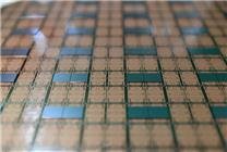
In an exciting development for the semiconductor industry, Taiwan Semiconductor Manufacturing Company (TSMC) has confirmed that its 1.4nm process, known as the A14 node, is scheduled for mass production in 2028. This announcement comes on the heels of the impending mass production of TSMC’s 2nm process, the N2 node, marking a new era in semiconductor technology.
Advanced Technology Features
The A14 node promises substantial advancements over its predecessor, featuring the second-generation Gate-All-Around Field-Effect Transistor (GAAFET) nanosheet architecture and a cutting-edge NanoFlex Pro unit architecture. These innovations will result in significant performance gains. TSMC claims that the A14 process could achieve:
- Up to 15% speed enhancement without increasing power consumption.
- A reduction in power consumption of up to 30% while maintaining the same performance levels.
- An increase in logic density exceeding 20%.
Notably, TSMC’s comparison of the A14 process is made against the N2 node rather than the transitional A16 process, underscoring the significant advancements anticipated with this new technology.
Milestones in Production
Mass production of the A14 is on track for 2028, as TSMC has recently filed applications with regulatory authorities to commence construction of a new facility dedicated to this process. The construction is expected to begin in Taichung by the end of the year, and the company is actively working to recruit skilled labor for this ambitious project.
To achieve the technological capabilities of the A14 node, TSMC is likely to employ High-NA EUV (Extreme Ultraviolet) lithography machines. These next-generation lithography machines come with a hefty price tag, approximately $400 million each—double that of current EUV machines priced at around $200 million. This substantial investment is part of a broader strategy, as TSMC anticipates spending around $49 billion (or roughly 350 billion yuan) to establish the necessary infrastructure for the 1.4nm chip production.
Economic Implications
With such significant investments, TSMC is looking to capitalize on its advanced manufacturing capabilities. Reports indicate that the foundry fee for the 1.4nm process may escalate to approximately $320,000 per wafer, up from the recently increased price of $30,000 for the 2nm process. If these trends continue, the manufacturing of 1.4nm chips could become prohibitively expensive for many companies outside of high-margin sectors.
Market Dynamics
The escalating costs associated with the A14 node could position companies like NVIDIA, which specialize in high-performance AI chips, as the primary beneficiaries. Contrastingly, mobile device manufacturers might struggle to afford the next-generation processors, and PC makers could find it increasingly challenging to produce CPUs and graphics cards that utilize the A14 process.
In light of these economic dynamics, the potential pricing strategies and market positioning will be crucial factors to watch as TSMC moves toward the implementation of its 1.4nm technology.
Conclusion
TSMC is on the brink of a new chapter in semiconductor manufacturing with its A14 1.4nm process set to debut in 2028. The technological advancements promised by this process, coupled with significant investment and expected increases in production costs, will undoubtedly reshape the landscape of the semiconductor market. As industries gear up for this evolution, the focus will shift to how companies adapt to these changes and leverage the enhanced capabilities offered by next-generation chip technologies.