Fudan University Achieves Breakthrough in Two-Dimensional Hybrid Flash Memory Technology
Summary:
- Fudan University has pioneered the world’s first two-dimensional silicon-based hybrid architecture flash memory chip, enhancing existing CMOS technology.
- Leveraging the integration of ultra-fast flash memory devices with mature semiconductor processes, this innovation is set to accelerate the development of high-speed information technology.
- The project aims to vastly improve chip yield and redefine the capabilities of memory devices in the coming years.
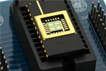
On October 9, Fudan University announced a significant leap forward in the realm of two-dimensional electronic devices. Following the introduction of "Dawn (PoX)" picosecond flash memory technology, the university has unveiled its novel "CY-01" architecture, merging cutting-edge two-dimensional ultra-fast flash memory with established silicon-based CMOS processes. This transformative hybrid architecture represents a landmark development in flash memory technology.
The team, led by Zhou Peng and Liu Chunsen, has made remarkable strides in overcoming the technical challenges associated with integrating these two-dimensional materials into existing CMOS frameworks. The research findings, featured in a recent article in Nature, clarify the full potential of this new chip architecture, asserting its ability to operate with remarkable efficiency.
A New Standard in Flash Memory Technology
Fudan University’s latest chip achieves a yield of 94.3% during testing, showcasing capabilities such as 8-bit instruction operation and high-speed 32-bit parallel processing. This new architecture not only meets but exceeds the performance of current Flash memory technologies, marking a pivotal moment for the industry.
Incorporating two-dimensional materials—which are just 1-3 atoms thick and remarkably delicate—into robust semiconductor designs has long been a daunting task. The existing methods often led to the degradation of the two-dimensional materials or poor circuit performance. To address this, the Fudan team pursued a strategy of modular integration, allowing the two-dimensional storage circuit to be fabricated separately before linking it to the CMOS control circuit through innovative high-density interconnections.
Engineering Innovations and Future Plans
Through meticulous engineering, the team achieved a near-atomic scale integration of two-dimensional materials with CMOS substrates. This groundbreaking process is pivotal in ensuring that the fragile materials maintain optimal performance, paving the way for the development of next-generation memory chips.
The advancements made by Fudan’s research team set the stage for further collaborations and experimental projects, with plans to elevate this technology to a megamagnitude scale within 3-5 years. This includes a focus on licensing the intellectual property developed during this research phase to industrial partners, thereby enhancing both academic and commercial ventures.
Conclusion: Redefining Future Electronics
Fudan University’s achievement not only signifies a major technological advancement but also provides a robust framework for the future of integrated circuit manufacturing. The integration of advanced two-dimensional materials with established CMOS technologies is poised to revolutionize the electronics landscape, ushering in a new era of high-speed, efficient information technologies.
This innovative approach demonstrates a commitment to advancing the field of electronics and lays a strong foundation for future explorations in memory device engineering. As the team continues their research, the implications of their work are likely to be profound, influencing various applications across the technology spectrum.