TSMC’s Cutting-Edge 2nm N2 Process Set for Mass Production in 2025
Summary:
- Mass Production Timeline: TSMC’s N2 process is slated to begin mass production in Q4 2025.
- Technological Advancements: The N2 technology promises significant improvements in transistor density and energy efficiency.
- Market Dynamics: AMD is set to leverage this technology in its upcoming Zen6 processors, marking a shift in priority away from Apple.
Taiwan Semiconductor Manufacturing Company (TSMC) is gearing up for a technological leap with its 2nm N2 process, expected to commence mass production by the fourth quarter of 2025. Official updates from TSMC indicate that this cutting-edge process will leverage nanosheet technology to enhance semiconductor performance and energy efficiency significantly.
Details of TSMC’s N2 Process
The N2 process represents TSMC’s first foray into Gate-All-Around (GAA) transistor technology, which is designed to achieve higher transistor densities and lower power consumption. According to the latest updates on TSMC’s website, significant advancements have already been realized:
- Increased Transistor Density: The new N2 technology boasts a 1.15x increase in transistor density compared to its predecessor, the N3E process.
- Power Efficiency: Power consumption is projected to decrease by an impressive 24% to 35%, while performance is expected to improve by up to 15%.
- Industry-Setting SRAM Density: The SRAM density has reached a staggering 37.9Mb/mm², establishing a new benchmark within the semiconductor industry.
Economic Considerations
The expenses associated with TSMC’s advanced N2 process are significant, with initial wafer foundry costs reported to exceed $30,000 per wafer, equivalent to over 200,000 yuan. Such pricing means that primarily large manufacturers will be able to invest in this technology.
Competitive Landscape
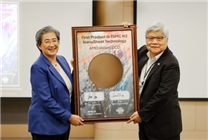
Traditionally, TSMC has prioritized customers like Apple for its new fabrication technologies, given their substantial financial backing and high demand. However, recent developments indicate a shift in dynamics. AMD, having announced plans for their sixth-generation EPYC processor—codenamed Venice—will be the first to utilize TSMC’s 2nm process technology. AMD’s CEO, Dr. Lisa Su, showcased the EPYC wafers alongside TSMC’s CEO, C. C. Wei, underscoring their collaborative partnership.
This shift suggests that while the iPhone 18 series was initially expected to be the first product utilizing N2 technology, AMD may take precedence, demonstrating the evolving priorities in the semiconductor marketplace.
Future Implications
The implications of TSMC’s N2 process extend beyond individual customers; they herald a new era of advanced computing. The efficiency and capability improvements are set to influence various sectors, including mobile computing, artificial intelligence, and cloud-based applications. As manufacturers adopt this next-generation technology, we can anticipate enhanced device performance, expanded battery life, and new functionalities that were previously unattainable.
In conclusion, TSMC’s N2 technology positions itself as a game changer in the semiconductor realm, setting us on a path toward advanced and efficient computing systems. With the mass production scheduled for late 2025, the industry watches closely as competitors adapt to this significant evolution in semiconductor technology.