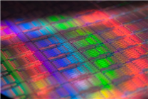
TSMC: The Unrivaled Leader in Advanced Semiconductor Technology
Summary:
- TSMC maintains a significant lead over competitors like Samsung and Intel in the semiconductor industry.
- The mass production of TSMC’s innovative 2nm and 1.4nm processes is set to reshape technology landscapes.
- Future advancements, including the 1nm process, are already in the pipeline, showcasing TSMC’s commitment to innovation.
As of January 15, TSMC (Taiwan Semiconductor Manufacturing Company) continues to hold a prominent position in the semiconductor landscape, despite emerging competition from giants like Samsung and Intel in the rapidly evolving 2nm node. While both companies have made strides, TSMC remains firmly established in key areas such as customer orders, capacity development, and technological advancements.
Competitors in Pursuit
TSMC’s CEO, Wei Zhejia, has expressed confidence in the company’s capabilities, stating that the depth of technological advancements creates a formidable barrier against competition. Even if Samsung or Intel announce breakthroughs in 2nm mass production, TSMC’s strategic developments are unlikely to be surpassed.
The 2nm Node Breakdown
The highly anticipated mass production of TSMC’s 2nm node, referred to as the N2 process, was initially announced in December. Production capacity is expected to start at 35,000 wafers per month, with projections to ramp up to 140,000 wafers by the end of the year—surpassing previous expectations. This new node will serve as the foundation for a variety of processes, including the enhanced N2P, which is slated for mass production later this year.
Moreover, the A16 node, essentially equivalent to a 1.6nm process, is part of the N2 family. Set to utilize innovative Super Power Rail (SPR) back power supply technology, A16’s production is also scheduled for this year, with NVIDIA poised to be its first customer. NVIDIA’s next-generation GPU, based on the Feynman architecture, is rumored to be the first to integrate this cutting-edge technology.
Future Innovations: The A14 and Beyond
Following the N2, TSMC is already looking ahead to the A14 process, designed to represent a significant upgrade with its second-generation Gate-All-Around (GAA) transistor technology. This process boasts impressive enhancements: a potential 15% increase in speed for the same power consumption or a 30% reduction in power consumption for comparable performance metrics, alongside a 20% boost in logic density.
Construction for the A14 production facility is progressing well, with machinery expected to be operational at the Baoshan P3 factory in Hsinchu by the third quarter of the year. Trial production is on track to begin in 2027, with mass production anticipated in the first half of 2028, targeting a capacity of 70,000 to 80,000 wafers per month.
Looking Further Ahead
The A14 family is expected to extend into more advanced processes, including A14P and A12, eventually leading to the development of the groundbreaking A10 process that aims to hit the 1nm milestone. Researchers face significant challenges, and mass production for this node is not expected until 2030.
Conclusion
With each breakthrough in semiconductor technology, TSMC proves its unwavering commitment to innovation and market leadership. As the race to miniaturize technology continues, TSMC’s strategic advancements not only secure its competitive edge but also pave the way for future developments that could reshape industries worldwide.
By remaining at the forefront of semiconductor innovation, TSMC is setting the pace for the industry’s future. As competitors strive to close the gap, TSMC’s robust technological foundation and visionary approach ensure it will remain a key player in the semiconductor arena for years to come.