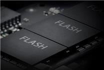
Samsung to Launch 3D Transistor Technology in Flash Memory Chips: A New Era of Efficiency
Summary:
- Samsung is set to implement 3D FinFET transistor technology in NAND flash memory chips, increasing performance and efficiency.
- This shift promises enhancements such as reduced power consumption, smaller chip sizes, and faster signal transmission.
- The exact models utilizing this technology have not been confirmed, pending further developments.
On October 23, it was reported that Samsung is poised to adopt advanced 3D FinFET transistor technology in its NAND flash memory chips, marking a significant evolution in memory chip design. This move signifies an important development in the semiconductor industry, following Intel’s pioneering introduction of Finfield transistors at the 22nm process node, which officially ushered logic technology into the 3D era.
FinFET, or Fin Field-Effect Transistor, features a unique three-dimensional structure that resembles a shark fin. This innovative architecture stands in stark contrast to traditional 2D planar transistors, offering numerous advantages that enhance overall performance. Intel was the first company to implement FinFET technology at the 22nm node, with TSMC and Samsung adopting it at the 14/16nm nodes. Today, the FinFET structure has become foundational for advanced semiconductor technologies.
For years, memory chips predominantly utilized conventional 2D transistor structures, but recent advancements signal a shift toward more sophisticated designs. At the SEDEX 2025 conference, Samsung’s Chief Technology Officer, Song Jae-hyuk, emphasized that to meet heightened expectations for performance and energy efficiency, a greater number of transistors must be stacked within a given area. The adoption of 3D FinFET technology stands out as a crucial innovation in this regard.
Samsung’s announcement indicates that its utilization of 3D transistor technology in NAND flash memory chips will be the first of its kind in the industry. This progresses towards significantly increasing both the storage density and performance of these memory devices. The integration of 3D transistors is expected to yield a range of benefits, including:
- Enhanced signal transmission speeds
- Reduced power consumption
- Compact chip sizes facilitating improved device design
While Samsung has laid the groundwork for this technological advancement, specific details on which flash memory products will incorporate 3D transistor technology remain unconfirmed. The commercialization phase is yet to be determined, as the company continues to refine its approach.
As the industry gravitates toward more efficient and effective transistor technologies, Samsung’s commitment to implementing 3D FinFET in its flash memory could redefine the landscape of semiconductor manufacturing. This evolution is not merely about enhancing existing products. It represents a leap toward next-generation devices that promise better performance and sustainability in an increasingly digital world.
In conclusion, Samsung’s foray into 3D transistor technology is set to innovate and elevate the NAND flash memory sector. As the market watches closely, the anticipated benefits of this transition could set new standards for efficiency and performance within the semiconductor industry.