Shanghai’s Breakthrough in Two-Dimensional Semiconductor Technology
Summary:
- The first domestic two-dimensional semiconductor engineering demonstration line has launched in Shanghai.
- Operated by "Yuanji Micro," this innovation aims to achieve silicon-equivalent 90nm processes by Q3.
- Two-dimensional semiconductors present a potential solution to Moore’s Law limitations in chip development.
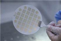
The landscape of semiconductor technology is witnessing a significant transformation. On January 8, Kuai Technology reported that the Shanghai Pioneer Industry Promotion Center announced the operational launch of China’s first domestic two-dimensional semiconductor engineering demonstration line. This groundbreaking initiative marks a crucial milestone for the semiconductor industry in China.
Developed by Yuanji Micro, an industry-university-research enterprise incubated at Fudan University, this demonstration line is expected to reach its line-through stage by June, with ambitions to achieve silicon-equivalent performance at a 90nm process node by the third quarter of this year. This advancement is crucial in an era where integrated circuits stand as one of Shanghai’s three leading industries.
The Promise of Two-Dimensional Semiconductors
Two-dimensional semiconductors represent the forefront of next-generation semiconductor technology. Their unique material characteristics—such as atomic thickness and high carrier mobility—offer substantial advantages over traditional silicon-based materials. These properties make two-dimensional semiconductors a potential key to overcoming the limitations imposed by Moore’s Law, which has recently shown signs of slowing down.
In contemporary applications, silicon-based chips are the standard; however, the shrinking size of transistors has made their manufacturing increasingly complex. This challenge can be visualized by likening silicon transistors to faucets, where electrons flow like water. As the "water pipe" narrows, the "inner wall" roughens, which diminishes the flow rate and overall efficiency.
In contrast, two-dimensional semiconductor materials maintain atomic-level thickness, effectively addressing issues such as "electron escape" that plague silicon-based chips. As the global competition intensifies, countries like the United States and members of the European Union are ramping up their investments in research and industrialization of two-dimensional materials, recognizing their potential to revolutionize chip manufacturing.
Fudan University’s Role in Innovation
Fudan University has established itself as a pivotal player in the research of two-dimensional materials, particularly in integrated circuit design, process iteration, and logic verification. The successful commissioning of Yuanji Micro’s demonstration line underscores the university’s commitment to fostering innovation across the entire technology spectrum—from fundamental research to applied studies and industrial applications.
Jin Li, the President of Fudan University, emphasized the institution’s leadership role in this domain, stating that the new micro-process line exemplifies its robust innovation capabilities. This full-chain approach to technological transformation ensures a strong foundation for future advancements in semiconductor technology.
Bao Wen, the founder of Weibo and a key figure in this initiative, revealed ambitious plans for the demonstration line. He stated, "We aim to leverage the capabilities of this demonstration line to achieve equivalent performance levels of 5nm or even 3nm silicon technology within the next 2 to 3 years, and we aspire to showcase solutions achieving 1nm equivalence within 4 years."
Broad Applications and Future Prospects
The implications of two-dimensional semiconductors are vast, extending into various high-tech fields, including:
- High-Frequency Communications: Enabling faster data transmission speeds and improved connectivity.
- Flexible Electronics: Offering new avenues for the development of bendable devices and wearables.
- Quantum Computing: Laying the groundwork for breakthroughs that could revolutionize computational capabilities.
As the semiconductor industry evolves, the ability to efficiently manufacture advanced chips at reduced sizes will be critical. The development of two-dimensional semiconductors holds the promise of significantly enhancing performance while addressing the limitations of current silicon-based technologies.
Conclusion
Shanghai’s new engineering demonstration line marks a pivotal moment for the semiconductor industry, positioning China at the forefront of two-dimensional semiconductor research and application. As developments continue, the future of chip technology and its wide-ranging applications remains promising, heralding a new chapter in the semiconductor landscape. With sustained investment and innovation, two-dimensional semiconductors could pave the way for revolutionary advancements in electronic devices, shaping the technological future for years to come.