NVIDIA’s Revolutionary GPU: The Feynman Architecture and the Integration of LPU for Enhanced AI Performance
Summary:
- NVIDIA is set to revolutionize AI inference with its upcoming Feynman architecture, integrating Language Processing Units (LPU) aimed at elevating performance.
- Utilizing advanced semiconductor technology, this new architecture will effectively address existing limitations in AI processing speed and efficiency.
- As NVIDIA pushes forward with this innovative design, challenges such as heat management and CUDA compatibility will need to be tackled for successful implementation.
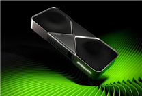
As the leader in AI training, NVIDIA is gearing up for a significant transformation in real-time reasoning. Plans are underway to introduce an innovative "secret weapon" that promises to reshape the industry landscape. The focal point of these advancements is the forthcoming Feynman architecture, which is poised to succeed its predecessor, the Rubin architecture.
Enhancements through LPU Integration
One of the standout features of the Feynman architecture is the planned integration of Language Processing Units (LPU) sourced from Groq. By incorporating these specialized units, NVIDIA aims to drastically improve AI inference capabilities, particularly in applications requiring instantaneous responses like voice dialogue and real-time translation.
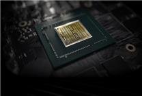
This advanced architecture will leverage TSMC’s cutting-edge A16 (1.6nm) manufacturing process. Notably, NVIDIA intends to utilize TSMC’s hybrid bonding technology to stack LPU units directly atop the GPU, a strategy aimed at optimizing performance while overcoming existing semiconductor constraints.
Innovative Design and Technological Synergy
NVIDIA’s design philosophy for the Feynman architecture draws comparisons to AMD’s 3D V-Cache technology. However, instead of conventional cache layers, NVIDIA focuses on integrating LPUs specifically tailored for inference acceleration. This strategic choice addresses the scalability challenges posed by SRAM within the constraints of extreme 1.6nm processes, which often result in high costs and space limitations when directly placing numerous SRAMs on the main chip.
By employing stacking technology, NVIDIA can maintain the core computing functionalities on the primary chip while allocating substantial SRAM requirements to supplementary stacked layers. This innovative approach envisions a future where NVIDIA GPUs can achieve unparalleled efficiency and speed, particularly during real-time data processing tasks.
Power Efficiency and Performance Gains
A salient feature of TSMC’s A16 process is its support for backside power supply technology. This breakthrough is expected to free up valuable chip space, allowing vertical signal connections to flourish. Consequently, stacked LPUs can communicate with the GPU rapidly while operating with minimal power consumption. The deterministic execution logic intrinsic to the LPU promises a substantial uptick in performance, translating to swifter AI responses.
Addressing Potential Challenges
While the advancements herald great promise, two critical challenges loom on the horizon: thermal management and CUDA compatibility. The addition of chip layers increases the density of computing components. Therefore, ensuring effective heat dissipation becomes paramount for NVIDIA’s engineering teams to avoid overheating scenarios.
Moreover, the deterministic execution order of the LPU necessitates precise memory configurations. The existing CUDA ecosystem, built on hardware abstraction, presents compatibility hurdles. Achieving seamless synergy between LPU’s execution model and CUDA’s framework will require sophisticated software optimization and engineering ingenuity.
The Future of AI Processing
As NVIDIA stands on the threshold of this groundbreaking transition, the implications for AI processing and real-time reasoning are profound. The integration of advanced technologies within the Feynman architecture marks a significant leap toward enhancing user experiences across a variety of fields from machine translation to interactive AI systems.
In a rapidly evolving landscape where the demand for immediacy in AI responses is ever-growing, NVIDIA’s vision could pave the way for next-generation applications that rely on instantaneous intelligence. By overcoming the inherent challenges presented by thermal management and software compatibility, NVIDIA is set to establish a new standard for AI performance and capability.
In conclusion, with the advent of the Feynman architecture and the innovative inclusion of LPUs, NVIDIA is poised to not only retain its competitive edge in AI training but also redefine the landscape of AI inference and real-time interaction. The next chapter in NVIDIA’s storied legacy promises to be just as transformative as its predecessors, emphasizing the importance of continual innovation in a fast-paced technological era.