ASML Revolutionizes Chip Manufacturing with New Photolithography Machine
Summary:
- ASML has delivered the "TWINSCAN XT:260," its first photolithography machine tailored for advanced packaging applications, enhancing 3D chip manufacturing capabilities.
- The XT:260 boasts significant advancements with a resolution of approximately 400 nanometers and a production speed of 270 wafers per hour, quadrupling the efficiency of previous machines.
- ASML anticipates robust business performance in the Chinese market, despite a projected decrease in demand from 2026 onwards.
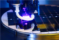
ASML, a leader in advanced semiconductor manufacturing technology, has recently announced the delivery of its first specialized photolithography machine, the TWINSCAN XT:260. This cutting-edge machine is designed to cater to the growing needs of advanced packaging applications, particularly in the 3D chip and Chiplet manufacturing sectors.
Advancements in Photolithography Technology
The TWINSCAN XT:260 aims to address the increasing complexity associated with chip packaging. As the semiconductor industry transitions toward 3D integration and novel chip architectures, the demand for larger exposure areas and higher throughput has never been more critical. This innovative machine utilizes i-line lithography, operating at a wavelength of 365 nanometers, yielding a resolution of around 400 nanometers. It boasts an impressive numerical aperture (NA) of 0.35, allowing it to process an astounding up to 270 wafers per hour—a productivity rate four times greater than existing advanced packaging lithography equipment.
Given these specifications, the XT:260 is particularly suited for interposer manufacturing, a vital process in integrating multiple chips into a single package. The machine features an exposure area of 26x33mm and employs a novel mask reduction technology that utilizes a two-fold reduction instead of the traditional four-fold. This improvement is strategically advantageous for interposer packaging applications, enhancing overall efficiency and effectiveness.
A New Chapter for ASML
While ASML has not disclosed the identity of the recipient for the inaugural XT:260, this delivery signifies a pivotal moment for ASML’s DUV deep ultraviolet lithography business. The company is poised to enter a new stage of operation, reinforcing its position as a technological powerhouse within the semiconductor sector.
In its recent financial report for the third quarter of 2025, ASML reported a net revenue of 7.516 billion euros, reflecting a slight year-on-year decline of 2.3%. The gross profit margin stood at 51.6%, a reduction of 2.1 percentage points from the previous year. Notably, ASML achieved a net profit of 2.125 billion euros, also exhibiting a year-on-year decrease of 6.4%. During this quarter, ASML sold 72 lithography machines, consisting of 66 new units and six reconditioned ones, representing a decline of four units compared to the previous year.
Future Outlook
ASML has highlighted a positive outlook for business performance in the Chinese market for 2024 and 2025, though anticipations signal a decline in demand from Chinese customers beginning in 2026, likely due to reaching a high baseline in sales volume.
This forward-looking approach emphasizes ASML’s commitment to innovation and responsiveness to market demands. The introduction of the XT:260 could position ASML not just as a supplier of machinery, but as a critical partner in the evolution of 3D chip technology and advanced packaging solutions.
In conclusion, the launch of the TWINSCAN XT:260 represents a significant advancement in photolithography technology, setting a new standard for chip manufacturing and packaging. With its groundbreaking features and enhanced productivity, ASML is likely to influence the semiconductor industry profoundly in the years to come. As the landscape continues to evolve, ASML remains at the forefront, driving innovation and meeting the challenges of an increasingly sophisticated market.
For those keeping an eye on the semiconductor industry, ASML’s latest innovations certainly warrant attention, as they promise to reshape the future of chip manufacturing with remarkable speed and efficiency.